Blog:
Adding USB-C to your Carrier Board Design - Part 2
This is part 2 of our 2-part blog post series. In part 1, you learned about USB-C pins, the configuration channel, and power distribution.
Let's continue by analyzing real-world examples using what you've learned, and then we'll wrap it up by analyzing the data signals on USB-C.
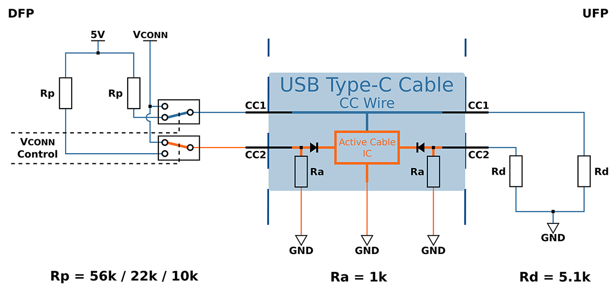
Before jumping into it, let's quickly recap the resistors setup and what are the possible detected states by the DFP Device (host) while monitoring the CC pins with different resistors connected:
| CC1 | CC2 | State | Cable Orientation |
| Open | Open | Nothing attached | N/A |
| Rp | Rp | Another DFP / No action | N/A |
| Rd | Open | Sink Attached | Normal |
| Open | Rd | Inverted | |
| Open | Ra | Powered cable without Sink attached | Normal |
| Ra | Open | Inverted | |
| Rd | Ra | Powered cable with Sink, VPA* or VPD** | Normal |
| Ra | Rd | Inverted | |
| Rd | Rd | Debug Accessory Mode Attached | N/A |
| Ra | Ra | Audio Adapter Accessory Mode Attached | N/A |
| *VPA - Vconn-Powered Accessory | |||
| **VPD - Vconn-Powered USB Device | |||
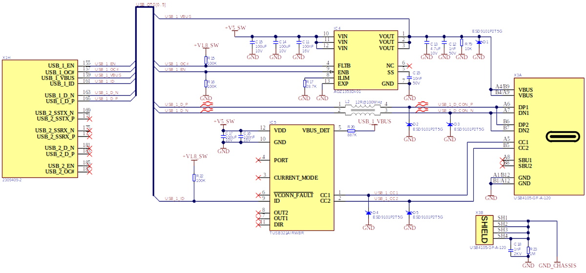
Now, you can benefit from checking a real working example - a dual-role USB-C port that is able to source power for an attached device.
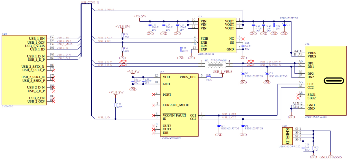
This section is taken from the Verdin Development Board and uses a chip TUSB321 for dealing with the configuration channel and a power-switching chip in the VBUS. The CC-connected chip detects the orientation of the cable and the presence of a sink device (see the table above). Then, it communicates the detected state to the Verdin module, which controls the power-switching chip. Depending on the strapping, the TUSB321 can announce different maximum output current levels (0.5/0.9A, 1.5A, and 3A). The current limit of the power-switching chip (IC4) needs to be adjusted accordingly.
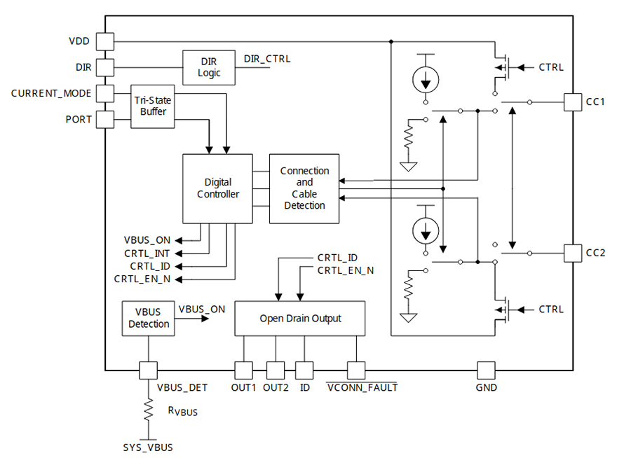
Within the TUSB321, you can see the CC pins switch to the pull-down resistor and a configurable resistance for the pull-up resistance. This arrangement enables your device to be used with UFP, DFP, and DRP configurations - set up by the PORT pin - and can be configured to announce its power delivery capacity - set up by the CURRENT_MODE pin. Since the TUSB321 only uses pull-up resistors for announcing the port's power capability, it can only announce 5V and 3A maximum (15W). For higher voltages, a configuration chip for advanced power delivery would be required.
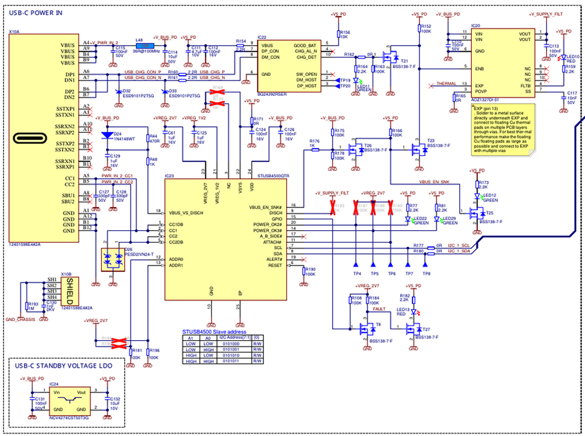
You will also find it helpful to have a look at a power sink device example.
This section is used on our Dahlia board, which has a chip (IC23) capable of doing bus communication. Therefore, this solution can negotiate for power profiles with higher voltages than 5V and currents higher than 3A. The chip connected to the CC pins has a built-in EPROM holding three profiles. This information is communicated via the CC bus and is used by the source device that responds with the available matching profile. When both devices agree on a mutually available profile, the VBUS is switched, and the device can start consuming power from the bus.
The schematics also feature an optional battery charger IC detector. This IC22 can detect the presence of a legacy wall power supply by checking whether the D+ and D- data signals are shorted together. If either the USB Power Delivery negotiation was successful (IC23) or a legacy USB Type-A battery charger is present (IC22), the bus power is enabled (IC20), and the board can start booting the module. If neither a battery charger nor a USB-C power delivery port is detected, the system will not start, as it is not allowed to draw more than 5V/100mA from the port.
The USB-C is notable for having significantly more data signal pins than the previous connector generations.
- Two lanes of Super-Speed signals - TX and RX pairs.
- Symmetrical pair of D+ and D- (redundant on the device sides only).
- Two Sideband Use (SBU) pins for special functions in alternate modes.
The USB 2.0 D+/D- pins are available rotation-symmetrically on the receptacle. That means there is no need to identify the orientation of the plugged cable and for a multiplexer for switching the signals.
To take advantage of the Super-Speed signal capabilities in USB-C, a multiplexer must be used along with the proper cable orientation detection using the CC pins - as explained in the first Blog - so the multiplexer can be controlled properly. This is needed to ensure that you are using the correct lane when using a dual or single-lane configuration.
Let's check real-world examples of how it all ties up together;
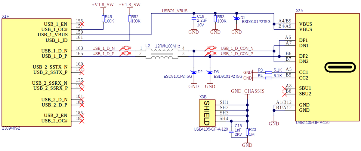
The simplest configuration to use the USB-C is as an upstream-facing High-Speed port device.
Using pull-down resistors in the CC pins and the D+ and D- pins, the circuit shown is a simple replacement of a Micro Type-B connector, and it's fully USB-C compliant. It can be used in devices such as mouse and thumb drives.
The OTG can be replaced with the configuration shown in the diagram below, from our Verdin Development Board, which was seen before in this blog post while analyzing the USB-C power source.
The CC pins and the already explained process for detection work for defining the behavior of the device - whether as DFP or UFP - and the D+ and D- pins are used for Data Signals in the same way as in the example before.
A good practice here is to use connectors without the Super-Speed pins populated since it greatly adds the density of pins, increasing the effort while routing the PCB.
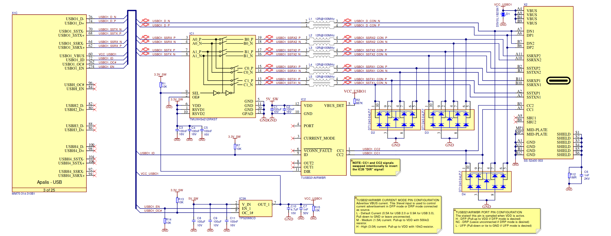
You can see a more advanced use of USB-C in our Apalis Carrier Board reference design.
When adding Super-Speed capabilities to your USB-C application, the multiplexer needed, as explained before, to connect the Super-Speed signals to the correct side of the cable can simply be controlled by the same TUSB321 chip.
In this design, a trick is used to facilitate the routing process: the CC pins are inverted, so the signal to control de multiplexer is inverted as well, simplifying the traces around the multiplexer.
Now, let's look at a full-feature example from a notebook-type application.
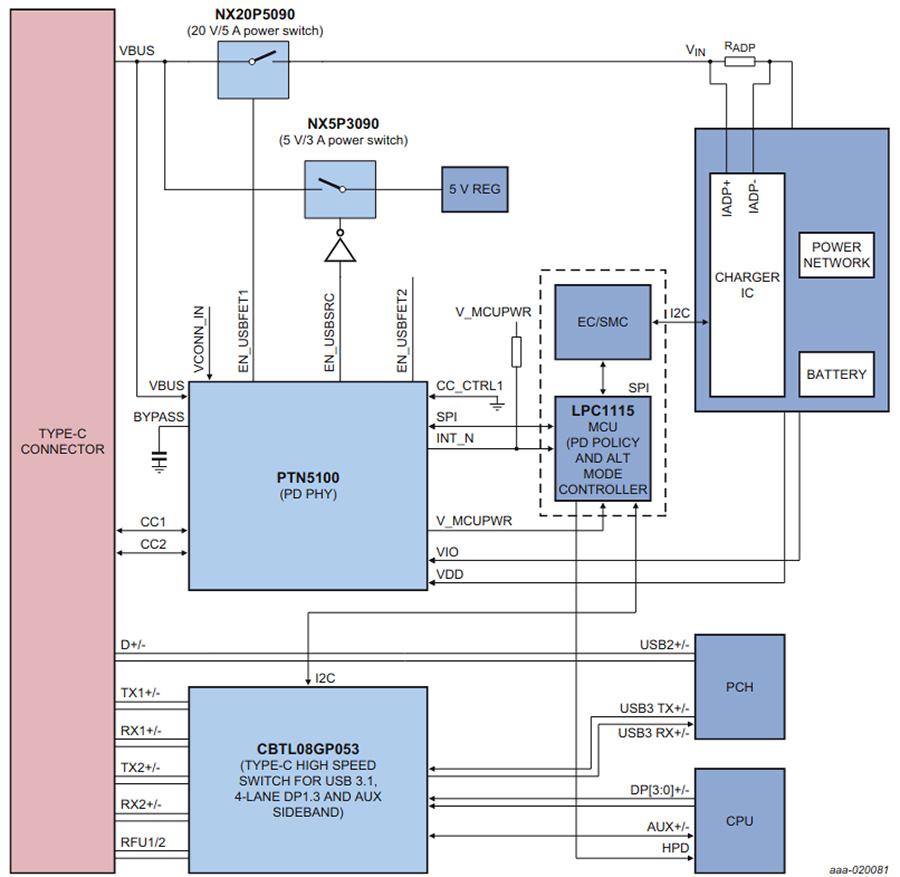
Laptop USB-C implementation
Source: https://www.nxp.com/docs/en/data-sheet/PTN5100.pdf
In this setup, the notebook can be charged or provide power to a UFP device, including power negotiation via a dedicated IC (PTN5100), and a simultaneous alternate function display port. Note the matrix switcher IC capable of connecting the video signals from the graphic part of the CPU and the Super-Speed signals coming from the south bridge of the system.
Let’s take a closer look at the possibilities with USB-C and display port configurations. You can see some of those options in the image below:
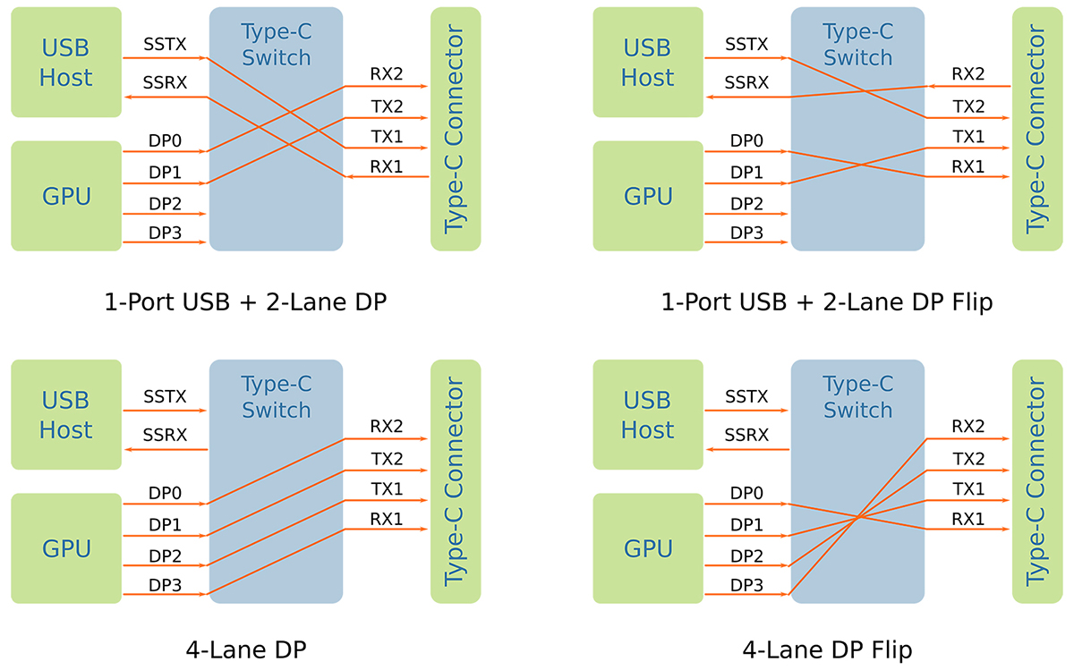
Display port configurations
It is important to know that display ports can run up to 4 lanes, but they can also use 1 or 2 lanes. Each bidirectional lane used for super-speed signals - RX/TX pairs - can accommodate 2 lanes for the display ports, since its lanes are unidirectional. Then, if you use just 2 lanes for the display ports, it's possible to use it in combination with super-speed signals in the remaining bidirectional lane. It also means that when using high resolution in the display port - which uses 4 lanes - you are limited to using 2.0 USB only with D+ and D- pins.
Let's check some mistakes that can be avoided by strictly following the standard.
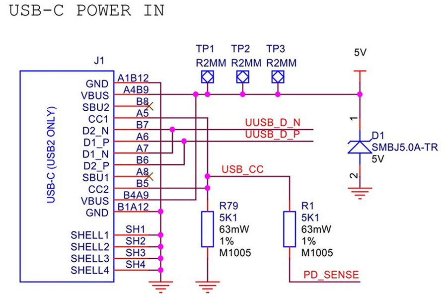
Rasp Pi 4 USB-C circuit
Source: https://datasheets.raspberrypi.com/rpi4/raspberry-pi-4-reduced-schematics.pdf
In the first revision of the Raspberry Pi 4, the CC pins shared the same Rd resistor - which caused them to be shorted together. When connected with passive cables - non-marked - the DFP device only senses Rd in one of the CC pins, since only CC1 via is routed in the cable, which results in a properly working power-sinking UFP device. Checking against the table:
| CC1 | CC2 | State | Cable Orientation |
| Rd | Open | Sink Attached | Normal |
| Open | Rd | Inverted |
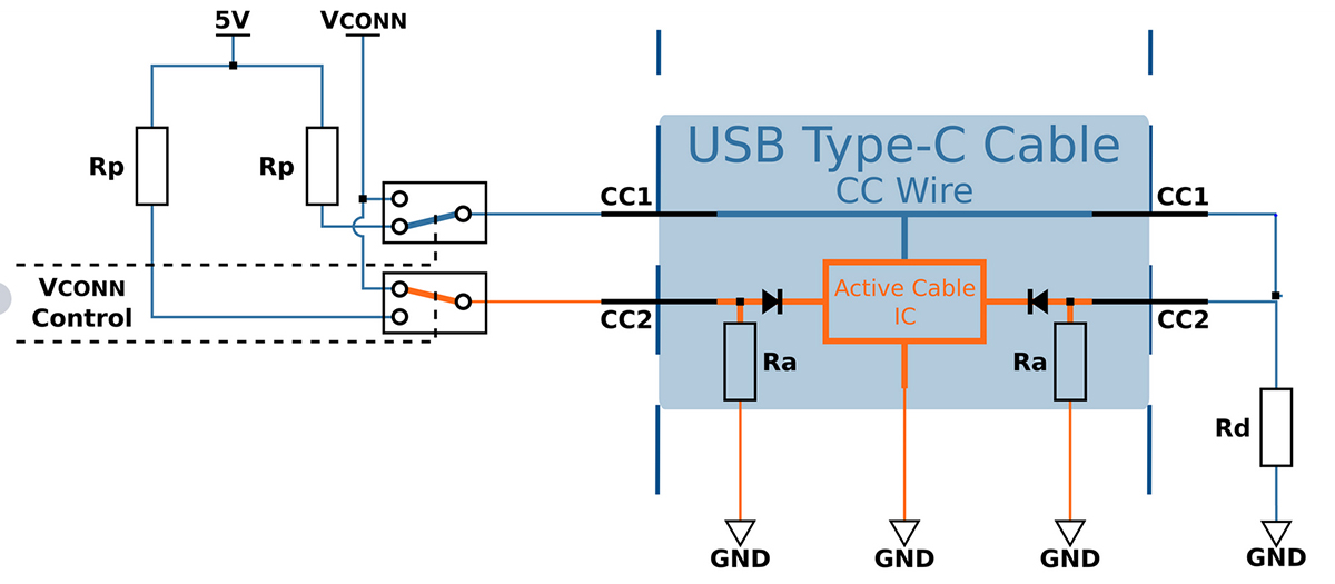
However, let's see what happens when it's connected to an active USB-C cable, which has a Ra resistor on each side of the CC2 line:
On the DFP device side, the CC2 pin senses the Ra resistor, and the CC1 pin senses the Rd resistor in parallel with the Ra resistor of the other end of the cable since the CC1 and CC2 pins are shorted on the Raspberry Pi board. This parallel configuration results in a resistance of 836 Ohms, which falls within the range of permitted values for Ra. If you carefully check the table again, you will see that this results in a state of audio adapter detected, leaving the board without power.
| CC1 | CC2 | State | Cable Orientation |
| Ra | Ra | Audio Adapter Accessory Mode Attached | N/A |
Having been introduced to basic USB-C concepts, you now know the possibilities it brings, its limitations, and the basic setup to use its resources.
More detailed information is available via the links below, and you are welcome to leave us a message if you need help with your carrier board design.
- Official USB Specifications https://www.usb.org/documents
- Wikipedia articles
- https://en.wikipedia.org/wiki/USB-C
- https://en.wikipedia.org/wiki/USB_3.0
- https://en.wikipedia.org/wiki/USB
- Short USB-C and Power Delivery Guide https://microchipdeveloper.com/usb:type-c
- Easy to read USB 2.0 - the basic about enumeration and the protocol https://www.beyondlogic.org/usbnutshell/usb1.shtml
- Toradex Design Guides
 Peter Lischer, Senior Hardware Developer, Toradex